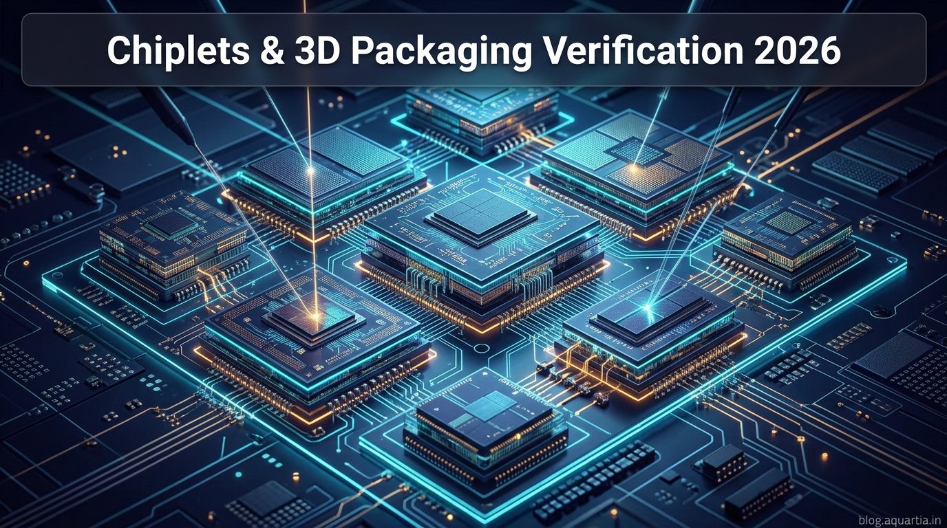
Monolithic single-die chips are hitting reticle limits and yield walls. In 2026, chiplets and advanced 3D packaging have moved from optional experiments to the primary architecture for high-performance AI silicon (Alpinum Consulting, TechInsights).
Packaging Is Now System Design
In modern multi-die packages—such as AMD’s MI455X combining separate compute (GCD) and memory (MCD) modules with 16 HBM4 stacks (LoveChip)—packaging directly dictates die-to-die latency, signal integrity, thermal dissipation, and manufacturing yield (Alpinum Consulting).
Why Verification Complexity Is Outpacing Design Complexity
- Cross-Die Interactions: Bugs now emerge at the boundary between third-party IP blocks, custom ASICs, and HBM stacks rather than inside isolated logic blocks.
- Agentic Verification: Teams increasingly use AI to generate testbenches and classify failures, but human engineering traceability remains mandatory before tape-out (Alpinum Consulting).
Frequently Asked Questions
Why are chipmakers adopting chiplets instead of monolithic dies?
Chiplets improve manufacturing yield, allow mixing different process nodes (e.g., 2nm logic with mature I/O dies), and scale memory bandwidth via 3D stacking.






+ There are no comments
Add yours