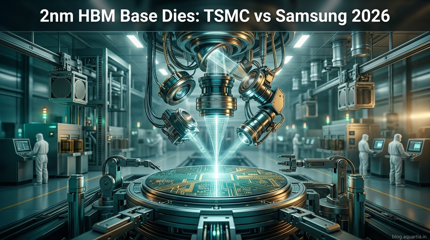
Historically, DRAM makers built the bottom “base die” of High Bandwidth Memory stacks using standard memory processes. Starting with HBM4 and HBM4E in 2026, that base die is becoming a sophisticated, logic-heavy interface—pulling leading-edge 2nm logic foundries directly into the memory supply chain (Medium / Tai Semicon, Shattered.io).
Custom Base Dies: Where Memory Meets Logic
Micron’s October 2026 roadmap highlighted custom HBM4E designs co-engineered with NVIDIA that place customer-specific logic IP directly into the base die using foundry processing (Shattered.io). Moving base dies to advanced nodes lowers I/O power consumption across the dozens of HBM stacks inside an AI server.
TSMC vs. Samsung Foundry Competition
- TSMC: Holds a commanding lead in leading-edge logic and advanced packaging, and NVIDIA has reportedly asked memory makers to use TSMC for NVHBM base dies (BigGo Finance).
- Samsung Electronics: Reportedly expanding its Taylor, Texas 2nm Fab 2 (2.7M sq. ft., targeting 2030 mass production) to win HBM base-die orders, leveraging its rare vertical integration across both DRAM and 2nm foundry (BigGo Finance, Medium / Tai Semicon).
Frequently Asked Questions
What is an HBM base die?
It is the bottom logic layer of a vertically stacked HBM cube that manages high-speed signaling, control, and data exchange between DRAM dies and the AI accelerator (Medium / Tai Semicon).







+ There are no comments
Add yours